美国网友问:中国能否发展出世界级的本土半导体产业?
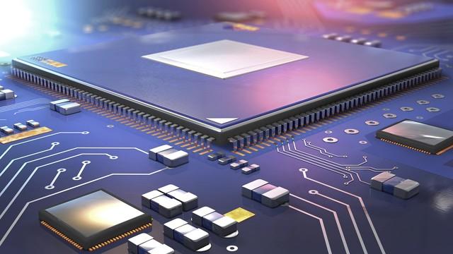
美国《芯片与科学法案》落地,决定对华禁售用于14nm以下先进制程工艺及制造相关设备,包括有“芯片之母”之称的设计软件EDA,意图阻止中国大陆获得高端芯片制造能力,还要求本土企业停止向中国出口用于人工智能工作的顶级计算芯片GPU,有业内人士称,美国此举意在“锁死中国人工智能发展的天花板”。在美版知乎Quora上,美国网友提问道:中国能否发展出世界级的本土半导体产业?我们看看各国网友的观点。

问题

美国网友西蒙•奎那汉的回答
This can be achieved, but not overnight, which requires a change of mindset.
这是可以实现的,但不是一蹴而就的,这需要改变心态。
I work for the world's fifth largest OSAT enterprise, engaged in outsourcing semiconductor (product) packaging and testing. We happen to have two factories in China. What products are they producing? Most products are based on lead frame, which is a very outdated packaging solution. This is the current reality in China. They use traditional packaging technology, but there is a serious lack of advanced packaging options.
我为世界第五大OSAT企业工作,从事外包半导体(产品)封装和测试,我们碰巧在中国拥有两家工厂。他们在生产什么产品?大多是基于引线框架的产品,这是一个非常过时的包装解决方案。这是中国目前的现实,他们用传统的包装技术,但严重缺乏先进的包装选择。
When I asked a colleague of semiconductor engineer about "advanced packaging", I was sure that there would be names like "InFO of TSMC", "Embedded Wafer BGA (eWLB) of Infineon" or "SWIFT of Amkor". But what about China? What advanced packaging IP can China's OSAT provide? I can only think of two: Huatian's eSiFO and Jiangsu Changdian's eWLB, which were acquired by Singapore STATS ChipPAC, and the latter was authorized by Infineon. Before purchasing STATS ChipPAC, Jiangsu Changdian had no advanced packaging capability. But if you ask me, I don't think this is a problem. Not all applications need the most advanced solutions. If they have the right mindset, they can catch up.
问一位半导体工程师同事有关“先进封装”的问题,我很肯定会出现“台积电的InFO”、“英飞凌的嵌入式晶圆级BGA(eWLB)”或“Amkor的SWIFT”等名称。但中国呢?中国的OSAT可以提供什么先进的包装IP?我只能想到两个:华天的eSiFO和江苏长电的eWLB,或是来自新加坡STATS ChipPAC的并购,或是由英飞凌授权的。在购买STATS ChipPAC之前,江苏长电还没有先进的封装能力。但如果你问我,我认为这不是什么问题,不是所有应用程序都需要最先进的解决方案。如果他们有正确的心态,他们可以赶上。
But what about foundries? I can say that they are advancing at an amazing speed. They have launched the 16nm process, which is one generation (or two generations) behind TSMC, but it is more than enough for most requirements of chip designers. For most consumer electronics, the performance difference between 16nm and 10nm is almost insignificant. It is generally believed that from 10nm to 7nm will require more effort and time than from 28nm to 16nm. Therefore, China should face relatively less difficulties in catching up with the wafer foundry industry, because the gap is getting smaller and smaller.
但晶圆代工厂呢?我可以说他们正在以惊人的速度前进。他们已经推出了16nm工艺,虽然比台积电落后一代(或两代),但对于芯片设计者的大多数要求来说,这已经绰绰有余。对于大多数消费电子产品,16nm和10nm之间的性能差异几乎不明显。人们普遍认为,从10nm到7nm将需要比从28nm到16nm更多的努力和时间,因此,中国在追赶晶圆代工行业方面应该面临相对较少的困难,因为差距越来越小。
I don't know much about IC design and software, but I want to say boldly: How difficult is it? 10 nanometer wafer process, wafer level packaging, ARM processor, and even iOS are all invented by human beings. They are not some foreign technology. There are more than 1 billion people in China shouting loudly. Finally, some people will come up with some solutions, which will remind me of my mentality.
我对IC设计和软件不太了解,但我要大胆地说一句:这有多难?10纳米晶圆工艺、晶圆级封装、ARM处理器,甚至iOS,它们都是人类发明的,它们不是某种外星技术。中国有超过10亿人口大声呼喊,最终有人会想出一些办法,这会让我想到心态问题。
It is no secret that the Chinese government is providing financial support for its semiconductor industry, but is the progress proportional to the funds that continue to flow into their pockets?
中国的政府正在为其半导体产业提供资金支持,这已经不是什么秘密了,但进展是否与不断流入的资金成正比?
But let's take a look at Qualcomm. Has the US government given them any funds for further research? No, but Qualcomm is the world's largest patent holder of RF technology.
但让我们看看高通公司,美国政府是否给了他们任何资金来进一步研究?不,但高通公司是世界上最大的射频技术专利拥有者。
My uncle went to China not long ago and visited a friend who worked in a Chinese science and technology company.
我叔叔不久前去了中国,拜访了一位在中国科技公司工作的朋友。
Uncle: You must be very happy to get the financial support from the state.
叔叔:能得到国家的金融支持你们一定很高兴。
Friend: Oh, yes, but we spent a lot of effort to finally use up all the money!Friend: Oh, yes, but we spent a lot of effort to finally use up all the money!
朋友:哦,是的,但我们花了相当多的努力才最终用光了所有的钱!
Uncle: So what achievements have you made this year?
叔叔:那么你今年取得了什么成绩?
Friend: I'm sorry, very few.
朋友:很遗憾,很少。
Uncle: That's unacceptable! What if the state stops subsidizing you and you have to bear the same amount of funds?
叔叔:那是不能接受的!如果国家停止资助你,而同样数额的资金需要你自己承担,该怎么办?
Friend: Then I am 100% sure that we will make a breakthrough in the short term.
朋友:那么我百分之百肯定我们会在短期内取得突破。
This is the mentality of China's semiconductor industry.
这是中国半导体行业的心态。
They have money, they have enough brains, but they lack motivation and competition.
他们有钱,他们有足够的脑力,但他们缺乏动力和竞争。
I believe that the science and technology war is an alarm for China. I think it is a good thing, because it is somewhat like Pearl Harbor, except that China is the United States this time. It will eventually give China's semiconductor industry a world-class impetus.
我相信贸易战对中国来说是一个警钟,我认为这是一件好事,因为它有点像珍珠港,除了这次中国是美国。它最终将给中国半导体行业成为世界一流的动力。

美国网友鲁伯特•拜恩斯的回答
Yes, in some parts of the value chain, we may see some world-class players gathered in a club, and the funds and prospects may attract global talents. Compared with the software industry, semiconductor engineers are generally underpaid. Therefore, except for the United States, China may be the only new player to invest a lot of money. You may see a large number of overseas Chinese engineers entering China to start their own businesses.
是的,在价值链的某些部分,我们可能会看到一些世界级的球员聚集在一个俱乐部里边,资金和前景可能会吸引全球人才。半导体工程师与软件行业相比,薪酬普遍偏低,因此,除了美国之外,中国可能是唯一一个投入大量资金的新玩家。你可能会看到大量海外华人工程师,进入中国创业。
But China will not be able to create a complete local industry. The semiconductor industry has been developed through decades of efforts and trillions of investment. IP barriers are very high, you can't cover all the subdivided fields.
但中国将无法创建一个完整的本地产业,半导体工业是经过几十年的努力和数万亿的投资发展起来的。IP壁垒很高,你不能包揽全部细分领域。
The semiconductor industry has a huge subdivision, which is itself a miracle of globalization.
半导体行业有一个巨大的细分领域,它本身就是一个全球化奇迹。
At the top of the value chain, we have American Lam Research, Applied Materials and Netherlands ASML, which provide the most advanced equipment. But there are not many in China.
在价值链的顶端,我们有美国Lam Research、Applied Materials和荷兰ASML,他们提供最先进的设备。但中国不多。
We have Shinetsu and Sumco from Japan, SK Siltronic from South Korea, and a few enterprises from China.
我们有日本的Shinetsu和Sumco,韩国的SK Siltronic,中国在方面的企业……不多。
Then from wafers to chipsets, we have Intel and Samsung. However, the largest wafer factory or chip manufacturer is TSMC, Taiwan's industrial crown jewel. China's SMIC International lags behind by about 2-3 generations. One of the bottlenecks is ASML, whose major shareholders are Samsung, Intel and TSMC. Therefore, SMIC is difficult to obtain the latest equipment even if it has professional technology and engineers.
然后从晶圆到芯片组,我们有英特尔和三星。但最大的晶圆厂或芯片制造商是台湾地区工业皇冠明珠台积电。中国的中芯国际落后约2-3代。其中一个瓶颈是ASML,其主要股东是三星、英特尔和台积电。因此,中芯国际即使拥有专业技术和工程师,也很难获得最新的设备。
In terms of logic, we have Intel, which produces its own chips, and AMD and Nvidia, which are designed but not produced. Does China have it? There are not many AI and Bitcoin mining machine design players with global competitiveness.
在逻辑方面,我们有生产自己芯片的英特尔,有设计但不生产的AMD和英伟达。中国有吗?除了一些具有全球竞争力的小众AI和比特币矿机设计玩家之外,这里再也不多了。
From our USB stick to iPhone storage, to cloud computing data center, Samsung, SK Hynix and Intel of South Korea dominate this market. China's own manufacturer YMTC is about two generations behind.
从我们的USB存储棒到iPhone存储,再到云计算数据中心,韩国三星、SK海力士和英特尔在这一市场占据主导地位。中国自己的制造商YMTC落后约2代。
In terms of mobile connectivity, the biggest competitor of 3G/4G LTE is Qualcomm, with MTK in Taiwan, China at the middle and high end, and Unigroup (Spreadtrum/RDA) in Chinese Mainland at the middle and low end. These are designers who usually use TSMC to make chips.
在移动连接上,3G/4G LTE最大的竞争对手是美国高通公司,中高端有中国台湾的MTK,中低端是中国大陆的Unigroup(展讯/RDA)。这些都是通常使用台积电制造芯片的设计师。

Now, we are moving towards the low-end of chip value chain testing and packaging, which is led by companies such as ASE/SPIL and Amkor.
现在,我们正朝着芯片价值链测试和封装的低端迈进,这是由ASE/SPIL和美国Amkor等公司主导的。
Therefore, as you can see from the above, semi industry is dominated by Americans and American military allies. After decades of integration, the barriers to entry for new entrants have become very high. Most sub industries are dominated by a few companies, which enjoy monopoly or oligopoly in their own "small" multi billion dollar market. Therefore, it is understandable that China, a late poor child, is trying to improve the value chain so that people can have higher income (which is almost the meaning of Made in China 2025), but it will be difficult for China to create a new ecosystem.
因此,正如你从上面看到的,半工业由美国人和美国军事盟友主导。经过几十年的整合,新进入者的进入壁垒变得非常高,大多数子行业由极少数公司主导,这些公司在自己的“小”数十亿美元市场中享有垄断或寡头垄断。因此,可以理解的是,中国这个迟到的穷孩子正在努力提升价值链,这样人们就能有更高的收入(这几乎就是《中国制造2025》的意义所在),但中国将很难创造一个全新的生态系统。
However, recent events have shown that globalization can be cut off by a few people, which will cause significant interference to the semiconductor supply chain, and this interference is bidirectional. Therefore, China may invest heavily in several key areas of the value chain to create a "multi-core assurance destruction" of the semiconductor version. Rare earths were once a part of it, but the United States is also rich in rare earths. Mining rare earths locally is too polluting and uneconomical.
然而,最近的事件表明,全球化可以被少数人切断,这会对半导体供应链造成重大干扰,而且这种干扰是双向的。因此,中国可能会在价值链中的几个关键领域进行大量投资,以打造半导体版本的“多核保证销毁”。稀土曾经是它的一部分,但美国也富含稀土,在当地开采稀土污染太大,不经济。
The following are the reactions of all parties:
以下是各方的反应:
Buyers of Chinese science and technology products: Damn it, will Americans cut off contact with China, so that I can't receive orders in time?
中国科技产品的买家:见鬼,美国人会切断中国的联系吗,这样我就不能及时收到订单了?
American: Damn, should I make this expansion plan now? The US government may block my sales?
美国人:见鬼,我现在应该制定这个扩张计划吗?美国政府可能会阻止我的销售?
Chinese: Americans can cut off our ties at any time. We'd better invest hard to replace at least some of them.
中国人:美国人可以随时切断我们的联系,最好努力投资,至少取代他们中的一些人。
Korean/Japanese: If we sell to China, Americans can stop us at any time. What should we do?
韩国人/日本人:如果我们卖给中国,美国人随时都可以阻止我们,我们该怎么办?
Student of School of Electrical Engineering: Yes, I don't need to turn to software engineering anymore. Maybe I should look for a job in China.
电气工程学院学生:是的,我再也不需要转向软件工程了,也许我应该在中国找工作。

中国网友丹尼尔•王的回答
Can China develop a world-class local semiconductor industry?
中国能否发展出世界级的本土半导体产业?
Yes, China can definitely develop a world-class semiconductor industry
是的,中国绝对可以发展出世界级的半导体产业
[1] Because semiconductor chips, as the source of rapid development of today's electronic information technology industry, have been widely infiltrated and integrated into various fields of national economy and social development, and are an important support for the development of China's digital economy and information consumption. Dr. Wen Xiaojun, the director and associate professor of CCID Group (subordinate to the Ministry of Industry and Information Technology) Information and Communication Technology Industry Research Institute, said that the 28 nanometer process will become a new starting point for 100% of domestic chips. It is expected that domestic 14 nanometer chips will be mass produced in 2021 and 2022 respectively.
[1] 因为半导体芯片作为当今电子信息技术产业快速发展的源泉,已经广泛渗透和融入国民经济和社会发展的各个领域,是我国数字经济和信息消费发展的重要支撑。赛迪集团(工信部下属)信息通信技术产业研究所所长、副教授温晓军博士表示,28纳米工艺将成为100%国产芯片的新起点,预计国内14纳米芯片将分别于2021和2022年大规模生产。
Although Chinese scientists and engineers face technical difficulties, the establishment of a world-class semiconductor industry in China has begun to become a reality.
尽管中国科学家和工程师面临技术困难,但在中国建立世界级半导体产业已经开始成为现实。
The development of 14 nm semiconductor industrial processing systems in China has overcome the following technical problems: key equipment such as etchers and thin film deposition have been developed from scratch and applied to large-scale production lines; Breakthroughs were made in the research and development of 14nm process; The results of subsequent packaging integration technology have been fully realized in large-scale production. Hundreds of key materials, such as polishing agents and sputtering targets, have passed the evaluation of large production lines and entered into mass sales. These achievements basically cover the entire industrial chain system of China's integrated circuit manufacturing system.
我国14nm半导体工业处理系统的发展克服了以下诸多技术难题:刻蚀机、薄膜沉积等关键设备从无到有,并应用于大规模生产线;14nm工艺研发取得突破;后续封装集成技术的成果已在大规模生产中得到充分实现。抛光剂和溅射靶等数百种关键材料已通过大型生产线的评估,并进入批量销售。这些成果基本覆盖了中国集成电路制造系统的整个产业链体系。
[2] To reverse the passive situation, it is necessary to introduce a whole set of technology from foreign companies.
[2] 扭转被动局面,需要从国外公司引进一整套工艺技术。
Behind every example that China can solve is the point where American technology has lost its political role. Too many American advantages will collapse. The US blockade of the semiconductor chip industry chain will collapse by 2024 at the latest. Under the positive cycle, it is estimated that by 2024, the localization of most semiconductor chips from raw materials, equipment, design, production and packaging can be solved in China.
在中国能解决的每一个例子背后,都是美国技术失去政治作用的点。太多的美国优势将崩溃。美国对半导体芯片产业链的封锁最迟将于2024年崩溃。在正周期下,预计到2024年,大部分半导体芯片从原材料、设备、设计、生产和封装的国产化都可以在中国解决。
The domestic 28nm production line will achieve 100% localization in 2021, thus changing the global semiconductor industry pattern.
国内28nm生产线在2021实现100%国产化,从而改变全球半导体产业格局。
[3] The rapid development of 14 nm or even 28 nm process localization means that Chinese people adopt a regression strategy and use mature technologies to meet the general chip needs first. The Chinese people do not blindly pursue a higher level of manufacturing technology, but pay more attention to design and packaging optimization, in exchange for the independent ability of semiconductor applications and the entire industrial chain.
[3] 14nm甚至28nm工艺国产化的快速发展意味着中国人采取回归策略,使用成熟的技术首先满足一般芯片需求。中国人并不盲目追求更高水平的制造工艺,而是更加注重设计和封装优化,以换取半导体应用和整个产业链的独立能力。
In addition, after the mass production of 14nm chips, the subsequent capacity expansion needs financial support, including lithography machines, cleaning equipment, polishing equipment and other required equipment. These equipment are not only expensive, but also consume a lot of water and electricity in the use process. It is necessary to integrate raw materials and parts suppliers, introduce customers in advance, and ensure that production capacity is fully utilized.
此外,14nm芯片量产后,后续的产能扩张需要资金支持,包括光刻机、清洁设备、抛光设备和其他所需设备,这些设备不仅昂贵,而且在使用过程中会消耗大量的水和电。要做好原材料和零部件供应商层面的整合,提前做好客户介绍,确保产能得到充分利用。
The 14-12nm generation production line is critical in current semiconductors. 14nm and above processes can meet the needs of 70% of the current semiconductor manufacturing processes, and the mid-range 5G chips are positioned using the 12nm process. In addition, 14nm can basically meet the manufacturing process requirements of domestic desktop CPUs in China.
14-12nm一代的生产线在当前的半导体中非常关键。14nm及以上工艺可以满足当前70%的半导体制造工艺的需求,中端5G芯片使用12nm工艺定位。此外,14nm基本上可以满足中国国产桌面CPU所需的制造工艺需求。
According to statistics, in the first half of 2019, the entire semiconductor sales market was about 200 billion dollars, of which 65% of the chips used 14 nm technology, only about 10% used 7 nm, and about 25% used 10 nm and 12 nm. It can be seen that 14nm has become the most widely used and marketable process technology. It has great development potential in AI chips, high-end processors and automobiles. The main applications include high-end consumer electronics, high-speed computing, low order power amplifier and baseband, AI, automobile, etc.
据统计,2019年上半年,整个半导体销售市场约为2000亿美元,其中65%的芯片使用14nm工艺技术,只有约10%的芯片使用7nm,约25%的芯片使用10nm和12nm。由此可见,14nm已经成为应用最广泛、最具市场价值的工艺技术。它在AI芯片、高端处理器和汽车方面具有巨大的发展潜力。主要应用包括高端消费电子、高速计算、低阶功率放大器和基带、AI、汽车等。
14nm technology is now booming in China. It has delivered a good report card, but if they want to control and achieve perfect catch up, it cannot be achieved overnight. The leading foreign manufacturer in the industry has many years of production experience in 14nm, and the depreciation of the production line has been completed. Chinese enterprises have no advantage in cost competition with these manufacturers. Therefore, there is a generation gap between China and world-class foundry companies in terms of technology catch-up. If they want to become latecomers, China needs to invest more human, financial and time costs.
14nm技术现在在中国蓬勃发展,它已经交出了一份不错的成绩单,但如果他们想控制并实现完美赶超,这不可能一蹴而就。该行业领先的外国制造商在14nm上拥有多年的生产经验,生产线的折旧已经完成。中国企业在与这些制造商的成本竞争中没有优势。因此,在技术追赶方面,中国与世界一流铸造公司之间存在着代沟。如果他们想成为后来者,中国需要投入更多的人力、财力和时间成本。
The integrated circuit industry is one of the world's leading industries, with super intensive capital, frequent replacement and extremely complex talents. It has higher technical difficulty, higher trial and error cost and difficulty in troubleshooting. It requires China to have the determination to develop independently, the perseverance to work hard, and the confidence to catch up with and surpass success. It also requires strong and continuous capital, iterative technology, qualified talents, and a market that integrates production and use to gather capital, technology, talents, and markets. These four elements work together to achieve successful catch-up and surpassing development.
集成电路产业是全球前沿产业之一,拥有超密集的资本、频繁的更替和极其复杂的人才。它具有较高的技术难度、较高的试错成本和故障排除难度。它要求中国有独立发展的决心、努力工作的毅力、赶超成功的信心,还需要强大和持续的资金、迭代的技术、合格的人才,以及一个集生产和使用于一体的市场,以聚集资本、技术、人才和市场。这四个要素共同努力,实现成功追赶和超越发展。
With the arrival of 5G and AIoT era, especially in the fields of smart cities, automatic driving, security and the Internet of Things, various products are increasingly rich. Chips are gradually focusing on the optimization of special scenarios, and special-purpose chips are about to usher in exponential potential. In the explosive era, the wide range of AIoT scenarios will also bring huge market space for 14nm process chips in China.
随着5G和AIoT时代的到来,特别是在智能城市、自动驾驶、安全和物联网领域,各种产品越来越丰富。芯片正逐渐专注于特殊场景的优化,专用芯片即将迎来指数级的巨大潜力。在爆炸时代,广泛的AIoT场景也将给14nm工艺芯片在中国带来巨大的市场空间。
The new high-resolution lithography machine that Chinese scientists began to build in 2012 can use ultraviolet light to etch circuit patterns smaller than 22 nanometers. Combined with other technologies, it can be used to make chips of about 10 nanometers in the future. China currently has 47 domestic patents and 4 international patents for new technologies. In fact, it is not that the Chinese cannot make their own lithography machine, but that it is difficult for Chinese scientists to bypass existing patents and create new things from scratch.
中国科学家于2012年开始建造的新型高分辨率光刻机可以使用紫外光蚀刻小于22纳米的电路图案。结合其他技术,它可以在未来用于制造大约10纳米的芯片。中国目前拥有47项新技术的国内专利和4项国际专利。事实上,并不是中国人无法制造自己的光刻机,而是中国科学家很难绕过现有专利从头开始创造全新的东西。

Gradually, Chinese scientists and engineers confidently achieved the goal of the Made in China 2025 project on time. In recent years, China's chip industry has maintained a rapid growth trend driven by factors such as increased self-sufficiency, specification upgrading and innovative applications. The development of semiconductor manufacturing capacity will take a long time, and it will take at least several years from project establishment to capacity realization.
渐渐地,中国科学家和工程师满怀信心地按时实现了中国制造2025项目的目标。近年来,中国芯片产业在自给自足程度提高、规格升级和创新应用等因素的推动下保持了快速增长的趋势。半导体制造能力的发展需要很长时间,从项目建立到产能实现至少需要数年时间。


评论